400G OSFP DD Dual LR4
Price: Rs 230341.59
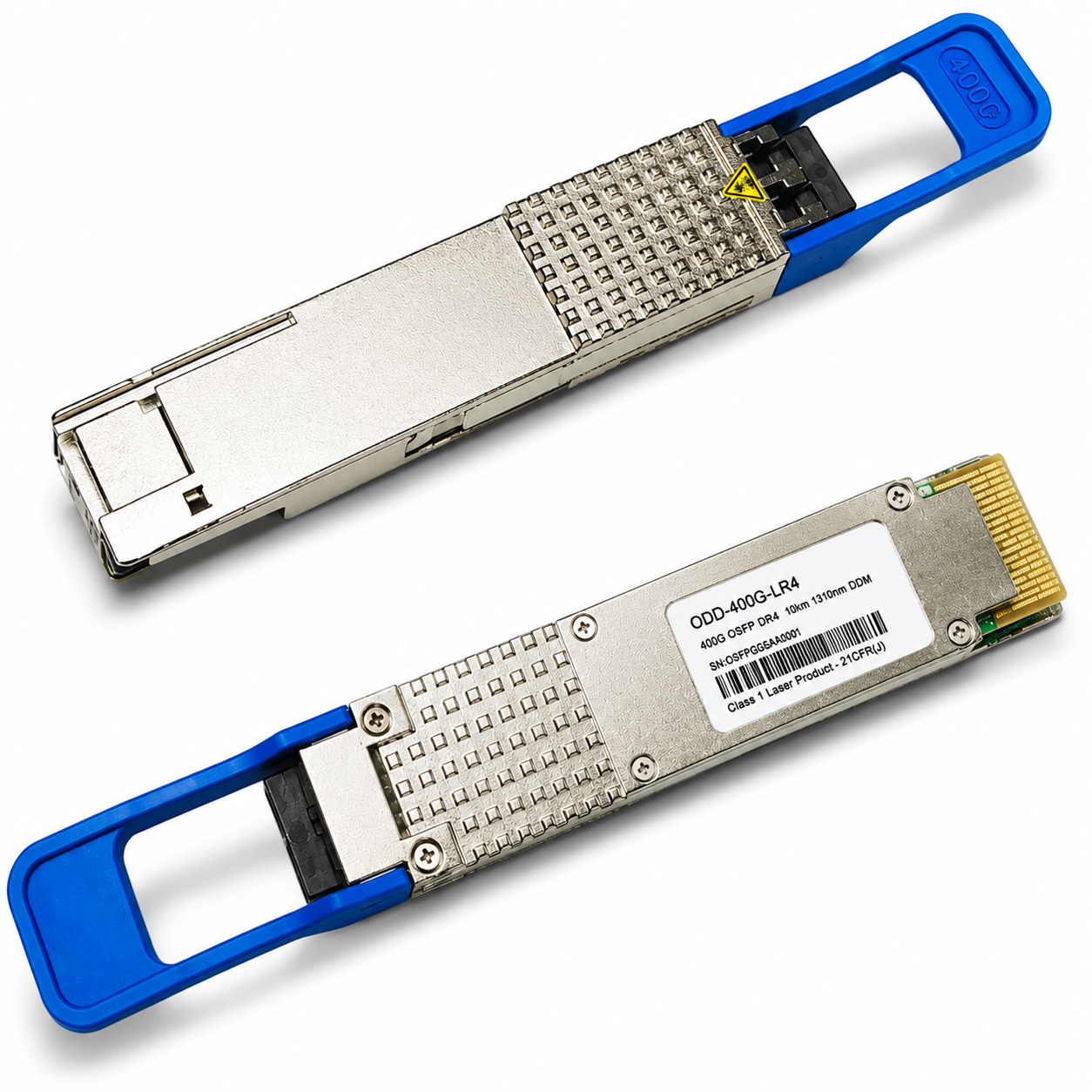
400G QSFP-DD LR4 Transceiver Module
400GBASE-LR4 • 10km-40km SMF • Duplex LC • QSFP-DD • CWDM4 • Low Power < 11W
The 400G QSFP-DD LR4 Transceiver Module is designed for high-speed 400G optical communication over single mode fiber. It supports transmission up to 10km using G.652 SMF with KP-FEC, making it ideal for data center interconnect, cloud networks, telecom backbone, and high-capacity enterprise optical links.
This module converts 8 channels of 50Gb/s PAM4 electrical signals into 4 channels of CWDM optical signals, delivering a total 400Gb/s optical output through a compact QSFP-DD form factor with duplex LC connector.
Data Rate
400G
Distance
10-40km
Connector
Duplex LC
Power
< 11W
Key Features
✔ QSFP-DD MSA and CMIS Compliant
✔ 400GBASE-LR4 Technical Specification
✔ 8 × 53.125Gbps PAM4 Electrical Interface
✔ 4 × 106.25Gbps Optical Architecture
✔ Up to 10km Over G.652 Single Mode Fiber
✔ CWDM4 Wavelengths: 1271 / 1291 / 1311 / 1331nm
✔ Built-in Digital Diagnostic Monitoring
✔ Low Power Consumption Less Than 11W
Product Description
The DT-400GDD-LR4 module is a cost-effective and low-power 400G QSFP-DD optical transceiver designed for 10km optical communication applications. It integrates EML drivers, EML lasers, optical multiplexer, de-multiplexer, DSP, and photodiode array to deliver reliable 400GBASE-LR4 performance for data center and telecom networks.
Applications
400G-LR4-10 Optical Links
CEI-56G-VSR-PAM4 Applications
Data Center Networks
Cloud Computing Infrastructure
High-Speed Backbone Links
Telecom Optical Networks
Recommended Operating Conditions
| Parameter | Symbol | Min | Max | Unit |
|---|---|---|---|---|
| Supply Voltage | Vcc | 3.13 | 3.47 | V |
| Operating Case Temperature | Tca | 0 | 70 | °C |
| Data Rate Per Lane | fd | 106.25 | 106.25 | Gbit/s |
| Humidity | Rh | 15 | 85 | % |
| Power Dissipation | Pm | — | 11 | W |
Electrical Specifications
| Parameter | Symbol | Min | Max | Unit |
|---|---|---|---|---|
| Differential Input Impedance | Zin | 90 | 110 | ohm |
| Differential Output Impedance | Zout | 90 | 110 | ohm |
| Differential Input Voltage | ΔVin | 900 | — | mVp-p |
| Differential Output Voltage | ΔVout | — | 900 | mVp-p |
| Bit Error Rate | BER | — | 2.4E-4 | — |
Optical Characteristics
| Parameter | Symbol | Min | Typical | Max | Unit |
|---|---|---|---|---|---|
| Centre Wavelength λ0 | λ0 | 1264.5 | 1271 | 1277.5 | nm |
| Centre Wavelength λ1 | λ1 | 1284.5 | 1291 | 1297.5 | nm |
| Centre Wavelength λ2 | λ2 | 1304.5 | 1311 | 1317.5 | nm |
| Centre Wavelength λ3 | λ3 | 1324.5 | 1331 | 1337.5 | nm |
| Side-mode Suppression Ratio | SMSR | 30 | — | — | dB |
| Average Launch Power | Pout | -2.7 | — | 5.1 | dBm |
| Receiver Sensitivity | RXsen | — | — | -6.8 | dBm |
| Average Receiver Power | Pin | -9 | — | 5.1 | dBm |
Regulatory Compliance
| Feature | Standard |
|---|---|
| Laser Safety | IEC 60825-1:2014, IEC 60825-2, EN 60825-1, EN 60825-2 |
| Electrical Safety | EN 62368-1, IEC 62368-1, UL 62368-1 |
| Environmental Protection | Directive 2011/65/EU with amendment (EU)2015/863 |
| CE EMC | EN55032:2015, EN55035:2017, EN61000-3-2:2014, EN61000-3-3:2013 |
| FCC | FCC Part 15, Subpart B, ANSI C63.4-2014 |
Ordering Information
| Part Number | Product Description |
|---|---|
| DT-400GDD-LR4 | QSFP-DD, 400GBASE-LR4, 10km on Single Mode Fiber, with DSP, power consumption <11W, duplex LC connector |
Note:
For stable 400G transmission, use high-quality G.652 single mode fiber, clean LC connectors properly, and confirm switch compatibility with QSFP-DD 400G LR4 modules before deployment.
For stable 400G transmission, use high-quality G.652 single mode fiber, clean LC connectors properly, and confirm switch compatibility with QSFP-DD 400G LR4 modules before deployment.