100G QSFP28 BIDI Tx1291nm/ Rx1311 nm
Price: Rs 152401.50
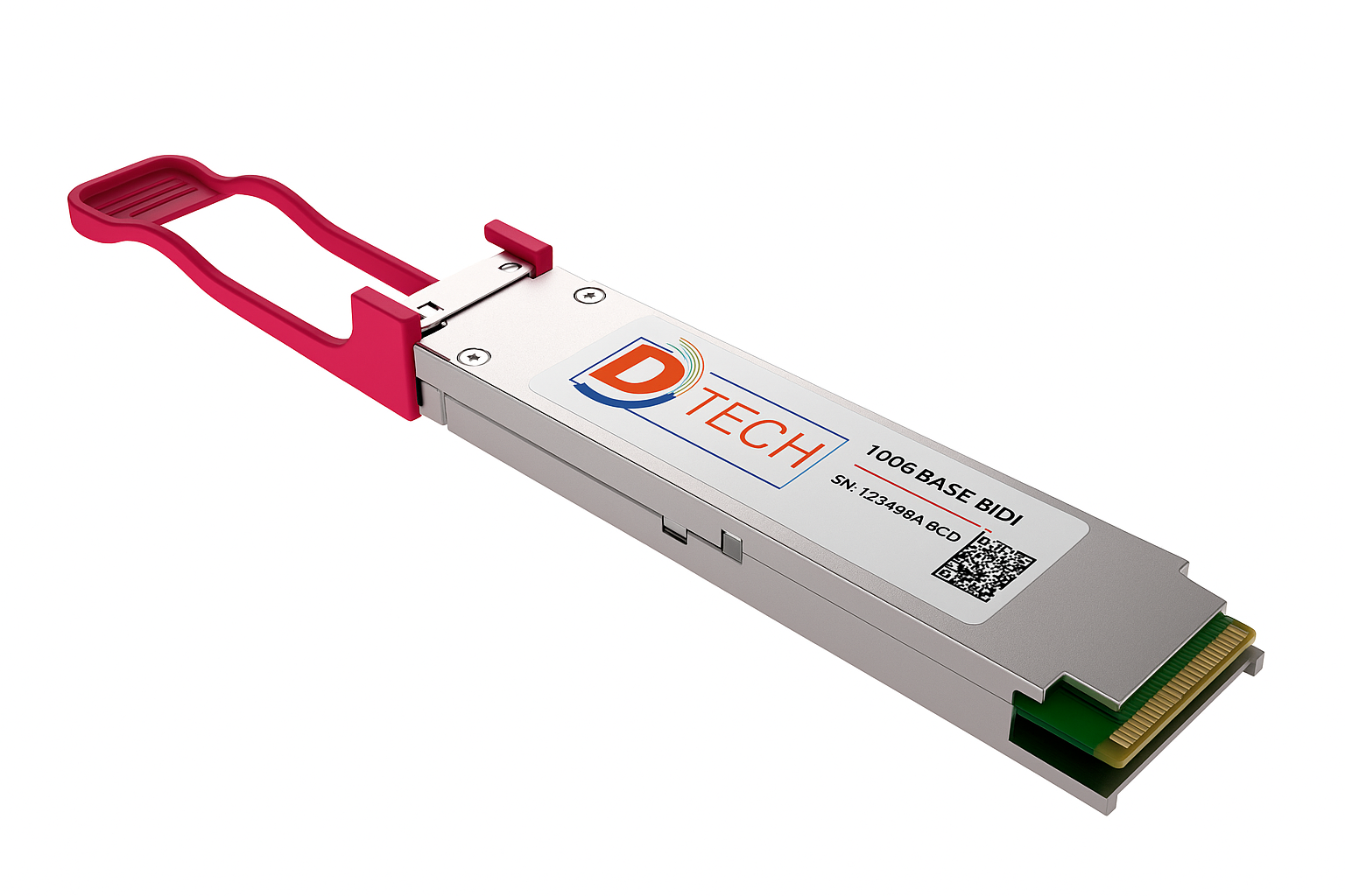
100Gbps Bi-Directional Simplex LC QSFP28 Transceiver
100G QSFP28 BIDI • 20KM Single Fiber • Simplex LC • Low Power <4W • DDM Supported
The 100Gbps Bi-Directional (BIDI) Simplex LC QSFP28 Transceiver is a high-performance optical module designed for 100G Ethernet, data centers, ISP backbone networks, enterprise fiber infrastructure, and telecom applications. It enables full-duplex 100Gbps communication over a single strand of single-mode fiber (SMF), reducing fiber requirements and lowering deployment costs.
Utilizing PAM4 modulation, EML laser technology, and an integrated PIN receiver, this module supports transmission distances up to 20 km. It features a simplex LC connector, integrated Digital Diagnostic Monitoring (DDM), low power consumption, and compliance with major QSFP28 industry standards.
Key Features
Applications
Technical Specifications
| Category | Specification |
|---|---|
| Product Type | 100Gbps QSFP28 Bi-Directional Optical Transceiver |
| Data Rate | 106.25Gbps PAM4 |
| Electrical Interface | 4 × 25.78Gb/s NRZ (CAUI-4) |
| Fiber Type | Single Mode Fiber (SMF) |
| Transmission Distance | Up to 20 km |
| Connector | Simplex LC |
| Laser Type | EML Laser |
| Receiver | PIN Photodiode |
| Operating Wavelength | Tx1291/Rx1311nm or Tx1311/Rx1291nm |
| Power Supply | Single +3.3V |
| Power Consumption | < 4W |
| Digital Diagnostics | DDM / DOM Supported |
| Operating Temperature | 0°C to +70°C |
| Compliance | SFF-8636, SFF-8679, QSFP28 MSA, 100G Lambda MSA, RoHS |
Ordering Information
| Variant | Laser Configuration | Distance | DDM | Latch Color |
|---|---|---|---|---|
| A | TX1291 / RX1311 | 20KM | Yes | Purple |
| B | TX1311 / RX1291 | 20KM | Yes | Red |
Digital Diagnostics Monitoring (DDM)
| Monitoring Parameter | Range | Accuracy |
|---|---|---|
| Temperature | 0°C to 70°C | ±3°C |
| Supply Voltage | 0 to VCC | ±3% |
| TX Bias Current | 0–100mA | ±10% |
| TX Optical Power | -0.2 to 6.8dBm | ±3dB |
| RX Optical Power | -10 to 6.6dBm | ±3dB |