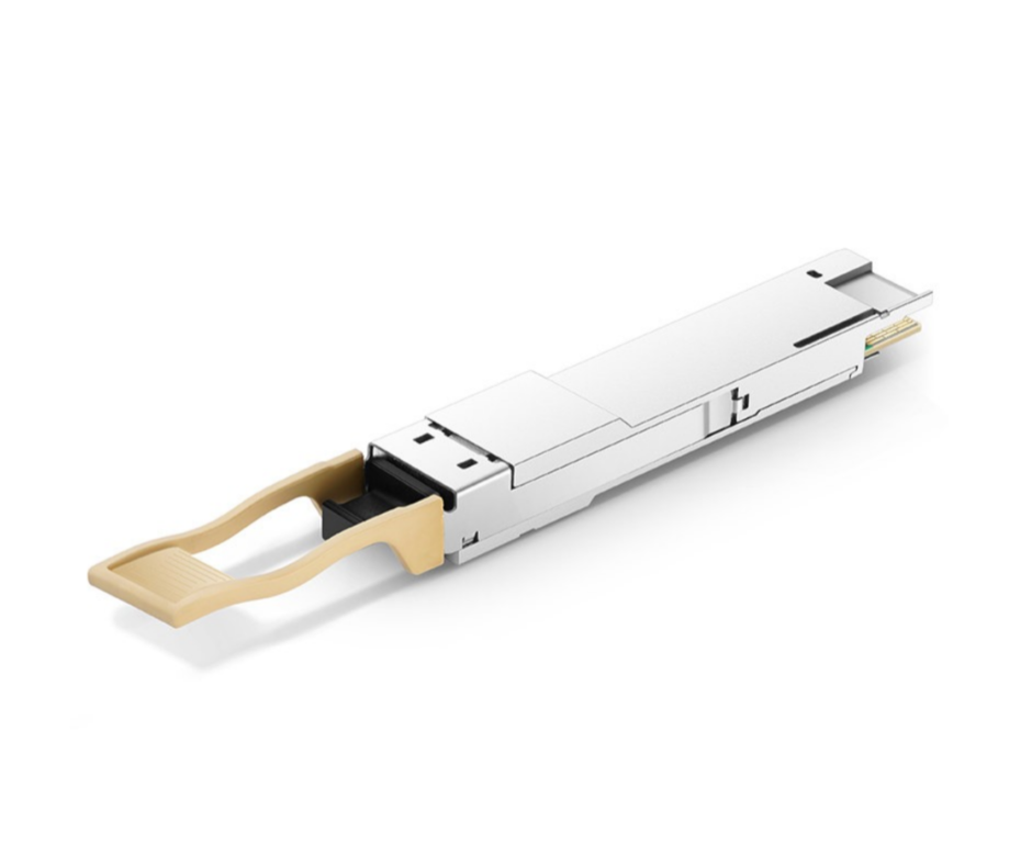
Important: BiDi modules work in pairs. Use Side A at one end and Side B at the other end of the fiber. RS-FEC (KR4-FEC) must be enabled on the host switch/router for 80km.
Product Features
- Supports line rate of 103.125 Gb/s
- Lane bit rate 25.78 Gb/s (100GE)
- Up to 80km transmission with KR4-FEC
- LAN-WDM EML laser and PIN receiver with SOA
- Supports multi-pin function with IntL/RxLOSL and LPMode/TxDIS
- High-speed I/O electrical interface (CAUI-4)
- I2C interface with integrated Digital Diagnostic Monitoring (DDM)
- QSFP28 MSA package with simplex LC connector
- Single +3.3V power supply
- Power dissipation: < 5.5W (Commercial)
- Complies with EU Directive 2015/863/EU (RoHS)
- Operating case temperature: 0 to 70°C
Applications
- 100GBASE-ZR4 Ethernet
- 100G Datacom & Telecom connections
- Long-distance links where fiber is limited (single-fiber 100G)
Description
The 100G QSFP28 ZR4 BiDi optical transceiver is designed for 80km optical communication over a single strand of single-mode fiber. It integrates the transmit and receive paths in one module.
On the transmit side, four lanes of serial data are recovered, retimed and passed to four laser drivers, which control four electro-absorption modulated lasers (EML) on the LAN-WDM grid. The four optical signals are multiplexed into a single-mode fiber through an industry-standard simplex LC connector.
On the receive side, the incoming optical signal is first amplified by an SOA (semiconductor optical amplifier), then an integrated optical demultiplexer separates it into four channels. Each channel is detected by a PIN photodetector and trans-impedance amplifier (TIA), retimed and passed to an output driver.
Side A transmits on 1273 / 1278 / 1282 / 1287 nm and receives on 1296 / 1300 / 1305 / 1309 nm; Side B is the reverse. The module features a hot-pluggable electrical interface, low power consumption and a 2-wire serial interface.
Wavelength Plan (Side A / Side B)
| Variant | TX Wavelengths (nm) | RX Wavelengths (nm) | Connector |
|---|
| Side A | 1273.55 / 1277.89 / 1282.26 / 1286.66 | 1295.56 / 1300.05 / 1304.58 / 1309.14 | Simplex LC |
| Side B | 1295.56 / 1300.05 / 1304.58 / 1309.14 | 1273.55 / 1277.89 / 1282.26 / 1286.66 | Simplex LC |
Absolute Maximum Ratings
| Parameter | Symbol | Min | Typ | Max | Unit |
|---|
| Storage Temperature | TS | -40 | | 85 | °C |
| Operating Case Temperature | TOP | 0 | | 70 | °C |
| Power Supply Voltage | VCC | -0.5 | | 3.6 | V |
| Damage Threshold, each Lane | THd | 5.5 | | | dBm |
| Relative Humidity (non-condensing) | RH | 0 to 85% | % |
Exceeding any of these values may immediately damage the device.
Recommended Operating Conditions
| Parameter | Symbol | Min | Typ | Max | Unit |
|---|
| Operating Case Temperature | Top | 0 | | +70 | °C |
| Power Supply Voltage | VCC | 3.14 | 3.3 | 3.47 | V |
| Maximum Power Dissipation | PD | | | 5.5 | W |
| Lane Bit Rate | – | | 25.78125 | | Gb/s |
| Transmission Distance | TD | | | 80 | km |
| Coupled Fiber | Single-mode fiber (9/125µm SMF) | 1 |
Optical Characteristics
| Parameter | Symbol | Min | Typ | Max | Unit |
|---|
| Transmitter |
| Signaling Speed per Lane | | | 25.78125 | | Gbps |
| Center Wavelength Lane 0 (Side A) | λ0 | 1272.55 | 1273.55 | 1274.54 | nm |
| Center Wavelength Lane 1 (Side A) | λ1 | 1276.89 | 1277.89 | 1278.89 | nm |
| Center Wavelength Lane 2 (Side A) | λ2 | 1281.25 | 1282.26 | 1283.27 | nm |
| Center Wavelength Lane 3 (Side A) | λ3 | 1285.65 | 1286.66 | 1287.68 | nm |
| Center Wavelength Lane 4 (Side B) | λ4 | 1294.53 | 1295.56 | 1296.59 | nm |
| Center Wavelength Lane 5 (Side B) | λ5 | 1299.02 | 1300.05 | 1301.09 | nm |
| Center Wavelength Lane 6 (Side B) | λ6 | 1303.54 | 1304.58 | 1305.63 | nm |
| Center Wavelength Lane 7 (Side B) | λ7 | 1308.09 | 1309.14 | 1310.19 | nm |
| Total Launch Power, 100GE | PT | 8 | | 12.5 | dBm |
| Average Launch Power per Lane | Pavg | 2 | | 6.5 | dBm |
| OMA, each Lane | POMA | 2 | | 6.5 | dBm |
| Launch Power Difference between any Two Lanes (Avg & OMA) | Ptx,diff | | | 3 | dB |
| Average Output Power (Laser Off) | Poff | | | -30 | dBm |
| Side Mode Suppression Ratio | SMSR | 30 | | | dB |
| Extinction Ratio, 100GE | ER | 8.2 | | | dB |
| RIN20OMA | RIN | | | -130 | dB/Hz |
| Optical Return Loss Tolerance | TOL | | | 20 | dB |
| Transmitter Reflectance | RT | | | -12 | dB |
| Optical Eye Mask | {0.25, 0.4, 0.45, 0.25, 0.28, 0.4} | % |
| Receiver |
| Signaling Rate, each Lane | | | 25.78125 | | Gbps |
| RX Wavelength Range (Side A) | λ0–λ3 | 1294.53 | 1295.56 – 1309.14 | 1310.19 | nm |
| RX Wavelength Range (Side B) | λ4–λ7 | 1272.55 | 1273.55 – 1286.66 | 1287.68 | nm |
| Damage Threshold, each Lane | Pdamage | 5.5 | | | dBm |
| Receiver Sensitivity (Average), each Lane | SEN | | | -26 | dBm |
| LOS Assert | LosA | -40 | | | dBm |
| LOS De-assert | LosDA | | | -28 | dBm |
Optical power launched into SMF. Measured with PRBS 231-1 at 25.78125 Gb/s, BER ≤ 5E-5.
Electrical Characteristics
| Parameter | Symbol | Min | Typ | Max | Unit |
|---|
| Transmitter (Module Input) |
| Data Rate, each Lane | | | 25.78125 | | Gbps |
| Differential Voltage pk-pk | Vpp | | | 900 | mV |
| Common Mode Voltage | Vcm | -350 | | 2850 | mV |
| Receiver (Module Output) |
| Data Rate, each Lane | | | 25.78125 | | Gbps |
| Common Mode Noise, RMS | Vrms | | | 17.5 | mV |
| Differential Output Voltage Swing | Vout, pp | | | 900 | mV |
| Eye Width | EW15 | 0.57 | | | UI |
| Eye Height | EH15 | 228 | | | mV |
| Differential Termination Resistance Mismatch | | | | 10 | % |
| Transition Time (20%–80%) | Trise/Tfall | 12 | | | ps |
Digital Diagnostics (DDM)
| Parameter | Unit | Accuracy |
|---|
| Temperature Monitor Absolute Error | °C | ± 3.0 |
| Supply Voltage Monitor Absolute Error | % | ± 5 |
| Bias Current Monitor Absolute Error | % | ± 10 |
| Received Power (Rx) Monitor Absolute Error | dB | ± 3.0 |
| Transmit Power (Tx) Monitor Absolute Error | dB | ± 3.0 |
Pin Definition
| Pin | Logic | Symbol | Description | Pin | Logic | Symbol | Description |
|---|
| 1 | | GND | Ground | 20 | | GND | Ground |
| 2 | CML-I | Tx2n | Transmitter Inverted Data Input | 21 | CML-O | Rx2n | Receiver Inverted Data Output |
| 3 | CML-I | Tx2p | Transmitter Non-Inverted Data Input | 22 | CML-O | Rx2p | Receiver Non-Inverted Data Output |
| 4 | | GND | Ground | 23 | | GND | Ground |
| 5 | CML-I | Tx4n | Transmitter Inverted Data Input | 24 | CML-O | Rx4n | Receiver Inverted Data Output |
| 6 | CML-I | Tx4p | Transmitter Non-Inverted Data Input | 25 | CML-O | Rx4p | Receiver Non-Inverted Data Output |
| 7 | | GND | Ground | 26 | | GND | Ground |
| 8 | LVTTL-I | ModSelL | Module Select | 27 | LVTTL-O | ModPrsL | Module Present |
| 9 | LVTTL-I | ResetL | Module Reset | 28 | LVTTL-O | IntL/Rx_LOS | Interrupt / Rx_LOS |
| 10 | | VccRx | +3.3V Power Supply Receiver | 29 | | VccTx | +3.3V Power Supply Transmitter |
| 11 | LVCMOS-I/O | SCL | 2-Wire Serial Interface Clock | 30 | | Vcc1 | +3.3V Power Supply |
| 12 | LVCMOS-I/O | SDA | 2-Wire Serial Interface Data | 31 | LVTTL-I | LPMode/TxDIS | Low Power Mode / Tx Disable |
| 13 | | GND | Ground | 32 | | GND | Ground |
| 14 | CML-O | Rx3p | Receiver Non-Inverted Data Output | 33 | CML-I | Tx3p | Transmitter Non-Inverted Data Input |
| 15 | CML-O | Rx3n | Receiver Inverted Data Output | 34 | CML-I | Tx3n | Transmitter Inverted Data Input |
| 16 | | GND | Ground | 35 | | GND | Ground |
| 17 | CML-O | Rx1p | Receiver Non-Inverted Data Output | 36 | CML-I | Tx1p | Transmitter Non-Inverted Data Input |
| 18 | CML-O | Rx1n | Receiver Inverted Data Output | 37 | CML-I | Tx1n | Transmitter Inverted Data Input |
| 19 | | GND | Ground | 38 | | GND | Ground |
GND is common for signal and power within the module; connect directly to the host board ground plane. VccRx, Vcc1 and VccTx must be applied together; each connector pin is rated for a maximum of 1000 mA.

.jpg)