
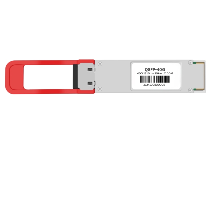
QSFP 40G LR4 1310nm Dual LC DDM
10km
Brand:
D-TECH
Variant Specifications
Compatible:
Warranty:
Weight:
Country of Origin:
Import Lead Time:
Package:
Warranty: 1 Year
Weight:
Country of Origin: China
More Details:
Import Lead Time:
Package:
1% OFF
Rs 16,601.77
List: Rs 16,725.66
40G QSFP+ ER4 1310nm Transceiver - 10km
The 40G QSFP+ ER4 optical transceiver is designed for high-speed 40G Ethernet transmission over single-mode fiber (SMF). It supports long-distance communication from 10km up to 60km, making it ideal for data centers, ISP backbone, and metro networks.
Key Specifications
| Parameter | Specification |
|---|---|
| Product Type | 40G QSFP+ ER4 Optical Transceiver |
| Data Rate | 41.25 Gb/s (4 × 10.3125 Gb/s) |
| Transmission Distance | 10 km / 20 km / 30 km / 40 km / 60 km (SMF) |
| Wavelength | 1271 / 1291 / 1311 / 1331 nm (CWDM) |
| Connector Type | Duplex LC |
| Fiber Type | Single Mode Fiber (9/125 µm) |
Optical Characteristics
| Parameter | Specification |
|---|---|
| Laser Type | CWDM DML Laser |
| Receiver Type | PIN ROSA |
| Launch Power (Per Lane) | 1 to 6 dBm (distance dependent) |
| Receiver Sensitivity | Up to –15 dBm |
| Optical Return Loss | ≥ 20 dB |
Electrical & Power
| Parameter | Specification |
|---|---|
| Power Supply | +3.3 V |
| Power Consumption | ≤ 4.5 W |
Monitoring (DDM)
| Supported Parameters | Module Temperature, Voltage, Bias Current, TX Power, RX Power |
Standards & Compliance
| QSFP+ MSA, IEEE 802.3ba (40G Ethernet), InfiniBand QDR/DDR/SDR |
Operating Temperature
| Commercial | 0°C to +70°C |
| Industrial | –40°C to +85°C |
Applications
- 40G Ethernet Networks
- Data Centers
- ISP Backbone & Metro Networks
- Enterprise Core Networks
Available Variants
- 40G QSFP+ ER4 – 10km
- 40G QSFP+ ER4 – 20km
- 40G QSFP+ ER4 – 40km
- 40G QSFP+ ER4 – 60km
Ask a question
Questions & answers
0 question(s)No questions yet. Be the first to ask!
0.0
5★
0
4★
0
3★
0
2★
0
1★
0
Write a review
Sign in to reviewCustomer reviews
No reviews yet. Be the first to review this product.
Product Videos
Watch demos, overviews and installation guides related to this product.
Related Products
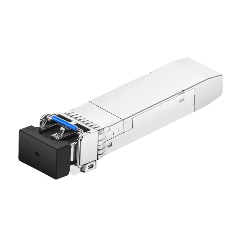
10G SFP+ 1310nm Dual LC
Rs 3,780
Rs 3,735
.jpg)
Face Plate / Wallplate
Rs 129
Rs 124
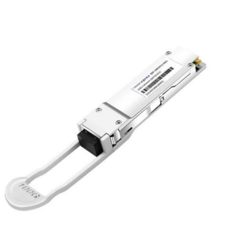
100G QSFP28 DCO DWDM C-Band LC Duplex SMF
Contact for price
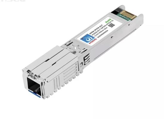
GPON OLT STICK
Rs 19,115
Rs 18,973
.png)
SFP 622M 1310nm Dual
Rs 2,700
Rs 2,668
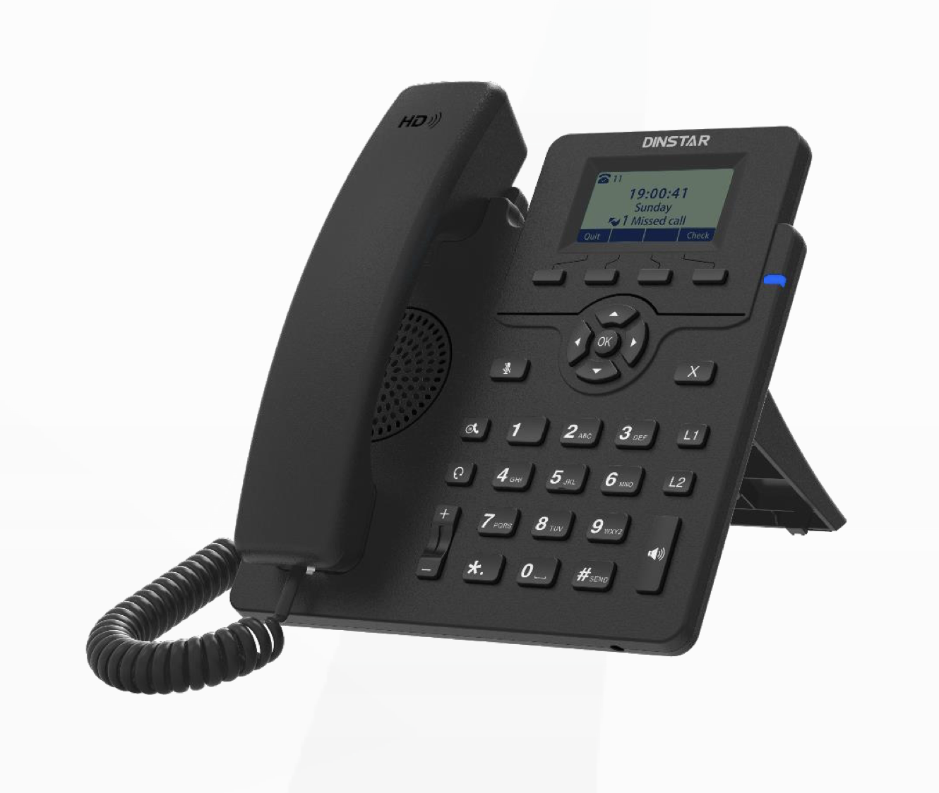
IP Telephone
Rs 10,000
Rs 9,999
.jpg)
HSGQ-X100GD
Contact for price
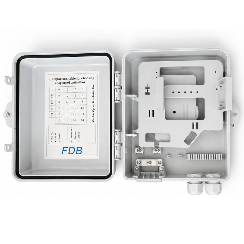
DB Box Heavy
Rs 1,434
Rs 1,417
.jpg)
HSGQ X200AXFD WIFI-6
Rs 5,000
Rs 4,900
.jpg)
IP-COM G2210P-8-102W
Rs 13,917
Rs 13,381
